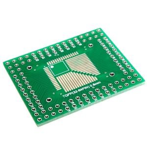
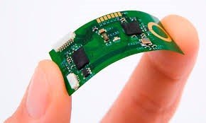
A fully operational PCB has to go through various development processes and phases before it can be used for the commercial purposes. The development processes involve the manufacturing of the Printed Circuit Boards (PCBs), designing of the integrated circuitry of the PCB on software which can be reproduced on the actual board and then finally the assembly of the components which involve the placing and soldering of the components on the Printed Circuit Boards (PCBs).
- Mechanical Manufacturing
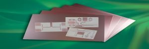
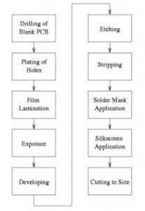
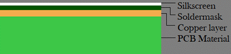
The Manufacturing of the Printed Circuit Boards (PCBs) involves the selection of material i.e. laminate and copper foil. Some of the most common materials used in the manufacturing of the Printed Circuit Boards (PCBs) are paper reinforced phenolic, paper reinforced epoxy, woven glass reinforced epoxy and Teflon material.
The properties of these materials vary from each other which make for selection possibilities depending upon the type of application the Printed Circuit Boards (PCBs) as to be used for. Paper reinforced epoxy materials are more suitable for Hole plating and have better electrical properties while the woven glass reinforced epoxy are transparent with shade of green and good water and moisture resistant properties. FR-5 series materials have better heat resistance properties and have higher Tg value as compared to material in other FR series.
Some of the properties which are commonly kept in consideration for the selection of material for the manufacturing of Printed Circuit Boards (PCBs) are greater cutting and drilling properties. The ability of material to withstand the application of chemical and acids is also given precedence during the material selection.
Another choice to be made in the manufacturing process of the Printed Circuit Boards (PCBs) is the thickness of the copper foil on the surface of the substrate. The copper thickness ranges from 17.5um to 105um. Some protective coating may also be applied on the surface of the copper foil to make it long lasting and durable.
The mechanical manufacturing hence involves the cutting of the Printed Circuit Boards (PCBs) into desired sizes and drilling where required. When the Printed Circuit Boards (PCBs) has been made into desired shape and copper foil has been deposited on its surface, the surface cleaning process takes effect. The surface cleaning is done with the help of chemicals like detergents, NaOH, Na2CO3 and surfactants.
- Software designing
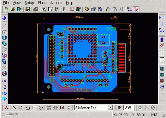
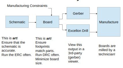
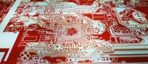
The second development stage for a PCB is the designing of the integrated circuit through the use of software which can give the Gerber Files i.e. the files outlining the copper foil tracks on the PCB and the Drill Files or Excellon files i.e. files which give details of drilling pattern on the Printed Circuit Boards (PCBs). The software designing is mostly done on PCB software like Altium, Proteus and CAD which give comprehensive computer aided designs.
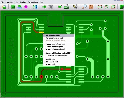
The Gerber files and drill files can be printed and iron on the surface of the Printed Circuit Boards (PCBs) or in a completely automated environment, they can be made use of by the designing machines where the patterns of the Gerber and drill files are etched on the surface of the Printed Circuit Boards (PCBs). The etching of the copper tracks on the PCB is done as per the software provided diagrams. The next step is the photo masking of drawing patterns on the Printed Circuit Boards (PCBs).
Once the tracks have been ironed on the surface of the Printed Circuit Boards (PCBs), the PCB is treated with oxidizing agent to remove the unwanted deposit of copper on the surface of the PCB. The most common oxidizing agents used are sulfuric acidic – hydrogen peroxide H2SO4 and ammonium-per sulfate (NH4)2S2O8. Ferric chloride and copper – tetrammin complex can also be used for the purpose of oxidation. The PCB is properly cleaned with the help of standard cleaning agents to make it ready for the drilling process.
The next stage of the PCB development is the drilling of holes as per the drilling file obtained from the computer aided design software. The drilling tools used are made of tungsten-carbide ranging in size from few micro meters to few millimeters. The size of the holes or via depends upon their type and application in the Printed Circuit Boards (PCBs).
- Printed Circuit Board Assembly (PCBA)
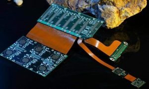
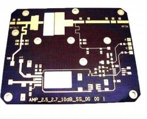
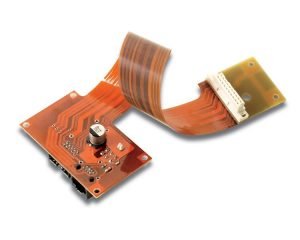
The Printed Circuit Board or the printed wiring board becomes a Printed Circuit Boards Assembly (PCBA) when the electronic components are placed on it on their designated places. The assembling process involves drilling of holes and via onto the Printed Circuit Boards for connections and placements of the components on the PCB, application of soldering paste, the application of surface mount technology for careful placing of the components on their designated paces, Reflow soldering for solidifying the connections made between the components and the soldering paste.
Once the connections have been made, the inspection and quality assurance tests are performed to trace and fix any fault in the assembly. Once the assembly is complete and quality assurance tests have been performed the Printed Circuit Boards assembly is than sent for final inspection and functional testing to analyze its testing under normal conditions under which it is supposed to work. If it gives positive results the product is then sent for the commercial use.
The basic steps involved in the Printed circuit board Assembly (PCBA) process is the application of solder paste on the surface of the board where soldering of the equipment will have to be required in the later stages of the process. The second stage is the placing of the components at their designated places with the help of standard mounting technology (SMT) as per the gerber and drill files pattern which dictate where the specific components are supposed to be placed.
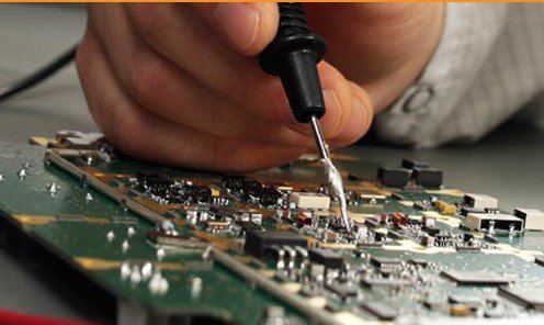
The next step in the assembly process is the reflow soldering where the assembly is heated at high temperature so as to melt the solder paste for embedding of the components on the PCB board. The final step in the assembly process is the quality inspection which involves various visual and operational tests to be performed in order to check the quality and standard of the printed circuit board.
At SynergisePCB inc. standard practices of PCB designing are made use in order to ensure the complete user satisfaction. All the processes of PCB manufacturing are carried out in United States of American under strict standards of quality. Our products are premium quality at very competitive rates.