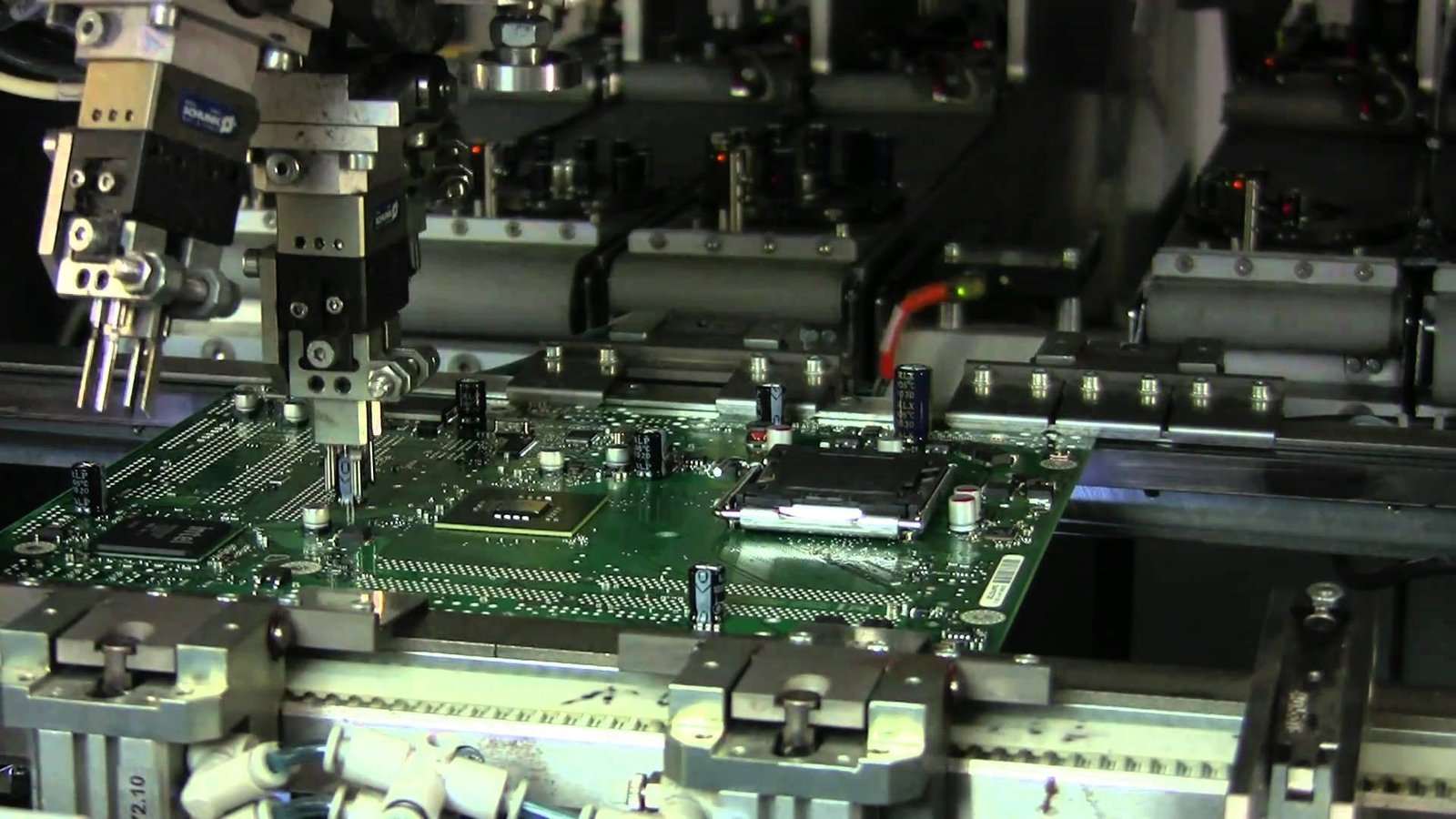
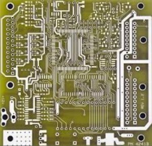
Printed Circuit boards (PCBs) are the core building blocks of most of the electronic items today and the drive for innovation and improvement in the operation and reliability of the modern electronic circuits is more powerful today than ever before. PCBs are used in all major applications from simple to highly complex integrated circuitry. Looking at this large range of application and dependence of the electronic devices of the Printed circuit boards, it wouldn’t be wrong to say that they PCBs drive the world of today. PCBs have reduced the size and weight of the conventional circuits while they have increased the design capabilities of the circuits manifold. They have paved the way for faster and more efficient processors to be built which require billions of transistors to be integrated on the board and work in unison. The high precision applications in aerospace technology and computer servers require the operation of integrated circuit of high density which has only been made possible through the advent of printed circuit boards.
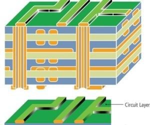
 Multi layer Printed Circuit Boards (PCB) has greatest and complex functional capability of all types of PCBs available today as they are used in wide range of consumer electronics i.e. smart phones and microwaves. Such devices tend to use Multi layer Printed Circuit Boards (PCB) for attaining less weight and small size. The multi layer PCBs are used in telecommunication devices such as transmission systems, GPS and satellite transmission systems. The reason behind using multi layer Printed Circuit Boards (PCB) in the telecommunication industry is the durability and high functionality provided by the multi layer Printed Circuit Boards (PCB).
Multi layer PCBs are also widely used in the medical industry due to the high density design capability made possible by them. In medical industry they are mostly used in x-ray machines, CAT scan, heat monitor devices and numerous other electronic devices used in the medical industry. Military and defense applications also widely use the multi layer Printed Circuit Boards (PCB) mostly in air traffic control systems, high power computers and servers operated in these environments, monitoring of sensors and wide range of military electronic devices.
The major reasons behind the wide use of Multi layer Printed Circuit Boards (PCB) is the high assembly density made available to the manufacturer. In Printed circuit board assembly it is given priority to choose the design such as to minimize the size and weight of the device, hence the multi layer Printed Circuit Boards (PCB) comes into play. The multi layer Printed Circuit Boards (PCB) also allow for controlled impedance features, greater EMI shielding and overall design quality which makes them most suitable for applications where smart designs are required.
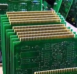
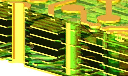
Multi layer Printed Circuit Boards (PCB) are like single or double layer Printed Circuit Boards (PCB) but in multi layer Printed Circuit Boards (PCB), the layers are substrate and copper coating exceed from two layers. The substrate of the multi layer Printed Circuit Boards (PCB) also range from glass epoxy resins to Teflon while the copper coating on the layers serves the purpose for drawing the conducting paths though the thickness of the copper coating can vary depending on the design and requirement of the application.
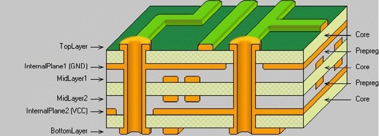
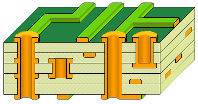
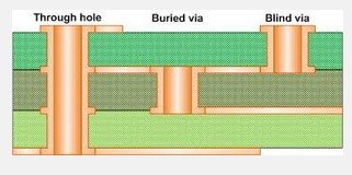
In Multi layer PCBs, the top and bottom layer contain the core between them which contain the inner layers stacked together. The different layers of the PCB are connected through via of various types depending upon the requirement. Some of the main types of via used in multi layer Printed Circuit Boards (PCB) are Plated through via, buried via hole and blind via hole.
1) Plated through Via
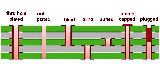
Plated through via connects the top and the bottom layer of the multi layer Printed Circuit Boards (PCB). In order to spot a plated through hole, you can see if the light passes through it or it is possible to see through it. Plated through holes are the simplest kind of holes and they only need drilling or laser light to be drawn. Drilling of plated through holes is relatively cheap but they may take up more space as compared with the other types of via or the micro via.
 2) Blind via hole (BVH)
Blind via hole connects the outer layer of the PCB with the inner layers and it is not possible to see through the Blind via Hole (BVH) which is the reason why it derives its name. Blind via Hole is mostly used where the size and space utilization of the Printed Circuit Boards (PCB) is of importance.
Blind via Hole are difficult to deal in as they require special attention to the depth of the hole to be made as anything imprecision in this regards can lead to severe design and operation complications. Due to the difficulty in handling them, the blind via Holes are not frequently used in the Printed Circuit Boards (PCB) assembly.
3) Buried Via Hole
The buried via Hole connects the inner layers of the Printed Circuit Boards (PCB) while it does not pass through the outer layer. The buried via holes are made use of where space utilization is important and high density applications are to be supported. The buried via holes are commonly used in HDI technology. Buried via holes are extremely difficult to work with as they require more time as compared with the blind via hole and the plated through hole technology while special care is required in working with them.
4) Micro Via
Micro via are another type of via used in the Printed Circuit Boards (PCB). They are via of very small size less than few micro meters and are used in highly sophisticated application. Micro-via are commonly used in flexible Printed Circuit Boards (PCB) or rigid flex Printed Circuit Boards (PCB).
Multi layer PCBs can be slightly costly as compared with the single layer PCBs which is only fair considering the high level design capabilities they are capable of supporting. They are also more complicated as compared with single layer PCB and skilled designers are required to work with them. At Synergize PCB Inc. we can provide Multi Layer PCB solutions up to 70L with our products complete manufactured in USA under the strict quality control standards. Our skilled working staff and cutting edge machinery can solve your complicated design requirements with your complete satisfaction.