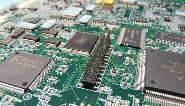
The Printed Circuit Board or the printed wiring board becomes a Printed Circuit Boards Assembly (PCBA) when the electronic components are placed on it on their designated places. The first step of PCB designing is the etching out of the copper tracks on the Printed Circuit Boards which involves the ironing of the designed print of the integrated circuit onto the board and then treating it with chemicals for the tracing of the tracks.
When the tracks are etched out on the Printed Circuit Boards the second stage of the PCB designing is assembling of the components. The assembling process involves drilling of holes and via onto the Printed Circuit Boards for connections and placements of the components on the PCB, application of soldering paste, the application of surface mount technology for careful placing of the components on their designated paces, Reflow soldering for solidifying the connections made between the components and the soldering paste.

Once the connections have been made, the inspection and quality assurance tests are performed to trace and fix any fault in the assembly. Once the assembly is complete and quality assurance tests have been performed the Printed Circuit Boards assembly is than sent for final inspection and functional testing to analyze its testing under normal conditions under which it is supposed to work. If it gives positive results the product is then sent for the commercial use.
Before the Printed Circuit Board assembly process begins, the DFM checks have to be performed in order to insure the suitability of starting the assembly process. The DFM checks cut cost by eliminating various unforeseen problems which may arise during the manufacturing process. An example of DFM process is to check if the conducting tracks are too close to each other which can cause serious design and operation problems at later stages. As part of our commitment to quality at Synergize PCB Inc we do DFM/DFA checks at every stage of the manufacturing and assembly of the Printed Circuit Boards.

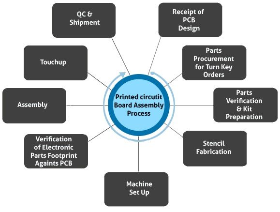
Process of Printed Circuit Boards Assembly
1) Application of Solder Paste
The first stage of the Printed Circuit Boards assembly is the application of solder paste on the surface of the PCB. The solder paste is applied only to certain places of the board i.e. where components are to be placed as per the design of the integrated circuit board. The solder paste is 96.5% tin, 3% silver and 0.5 % copper in composition and is little metal ball in shape. The solder paste is applied with a flux which helps the solder paste melt and bond to the surface. The application of solder paste is done through a machine which spreads the paste across the evenly to the designated area.
2) Placing of the Components (SMT)
After the application of solder paste to the surface of the PCB has been completed, the board moves to the pick and place machine where the components are placed by the machine to their designated places. The surface mount technology is used here which has replaced the manual method of placing the surface mount components (non connector type components) with the help of tweezers. The machine moves and directs the Printed Circuit Boards to help the process of components to their designated positions.
3) Reflow Soldering
The third step in the assembly process of printed circuit boards is the reflow soldering process in which the soldering paste is heated to be melted and solidified again so as to affix to components to their designated places. After the pick and place process has been completed, the PCB is shifted to the reflow section where board is heated to high temperature of around 250C which melts the solder in the solder paste. Once the solder paste melts, the components placed on it gets affixed to their designated places.
4) Inspection and Quality Control
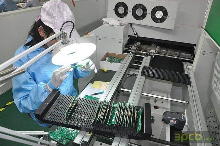
The fourth step in the Printed Circuit Boards assembly process is the inspection and quality control of the PCB. During this stage various inspection tests are performed to analyze the quality and operation capability of the PCB. One of the inspection tests is the manual check though this only done for small quantity inspections and its results are not highly reliable.
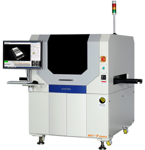
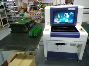
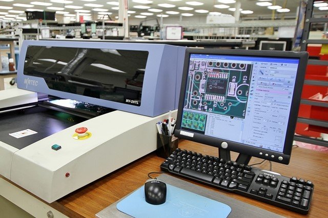
a) Automatic Optical Inspection (AOI)
The standard technique of inspection of the PCB assembly is the automatic optical inspection which is done with the help of AOI machine. The AOI machine makes use of high resolution cameras to check the PCB for faults in design and assembly. It also checks for defects in the tracks and the soldering on the board.
b) X-Ray Inspection
The less common method of inspection is the x-ray inspection and used only for layered PCBs. The x-ray inspection allows seeing the inner layers of the PCBs and any problem which may be associated with them.
5) Final Inspection and Functional Test
The final inspection tests are performed in which the PCB is tested for operation under normal conditions in which it is supposed to work and the performance profile is established. If the performance profile comes good the Printed Circuit Boards is recommended for operation, otherwise the Printed Circuit Boards is either sent for repair or scrapped as per the recommendations. All in all the testing phase is the most important phase in the manufacturing and assembly phase of the PCB.
At Synergize PCB Inc. we put great stress at the efficient and reliable working of the Printed Circuit Boards and all assurance of quality are provided to our customers.