When you are working on a university or college project maybe designing a simple power supply or doing a project with servo motors control, you may want to design the printed circuit board (PCB) for the electronic circuitry in order to bring neatness to your work. The printed circuit board can solve the issue of size and weight in case you are working on a cod copter or hove-craft project. In these cases the wiring weight associated with the conventional circuits gets very reasonable for deciding the motor ratings. When working on a small scale project, you can design and manufacture your own printed circuit board prototype though in case of more complicated projects and large scale manufacturing, you can see the assistance of SynergisePCB Inc. team at USA, Chicago.

In this Do-It-Yourself tutorial we will learn how to design a simple printed circuit board in your own college or university laboratory.

What Stuff will you need?
In designing the printed circuit board own your own, there are some important things that you will need. A list of the items required is given below,
- A copper clad printed circuit board
- Fine Grain Sand Paper
- Iron
- Muriatic Acid
- Hydrogen peroxide
- Disposable container for containing the acid.
- PCB handler
- Water Sink
- Power supply
- Wash Cloth for cleaning PCB
- PC having the PCB software
- Printer
- Solder

Some safety equipment is also recommended while working with the PCBs as it involves working with acids and hot iron.
The second development stage for a PCB is the designing of the integrated circuit through the use of software which can give the Gerber Files i.e. the files outlining the copper foil tracks on the PCB and the Drill Files or Excellon files i.e. files which give details of drilling pattern on the Printed Circuit Boards (PCBs). The software designing is mostly done on PCB software like Altium, Proteus and CAD which give comprehensive computer-aided designs.

The Gerber files and drill files can be printed and iron on the surface of the Printed Circuit Boards (PCBs) or in a completely automated environment, they can be made use of by the designing machines where the patterns of the Gerber and drill files are etched on the surface of the Printed Circuit Boards (PCBs).

The etching of the copper tracks on the PCB is done as per the software provided diagrams. The next step is the photo masking of drawing patterns on the Printed Circuit Boards (PCBs). Once the tracks have been ironed on the surface of the Printed Circuit Boards (PCBs), the PCB is treated with oxidizing agent to remove the unwanted deposit of copper on the surface of the PCB. The most common oxidizing agents used are sulfuric acidic – hydrogen peroxide H2SO4 and ammonium-per sulfate (NH4)2S2O8. Ferric chloride and copper – tetramin complex can also be used for the purpose of oxidation.

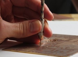
The PCB is properly cleaned with the help of standard cleaning agents to make it ready for the drilling process. It requires extreme care in drilling holes as this process can damage is PCB if not done right.
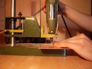
The next stage of the PCB development is the drilling of holes as per the drilling file obtained from the computer aided design software. The drilling tools used are made of tungsten-carbide ranging in size from few micro meters to few millimeters. The size of the holes or via depends upon their type and application in the Printed Circuit Boards (PCBs).
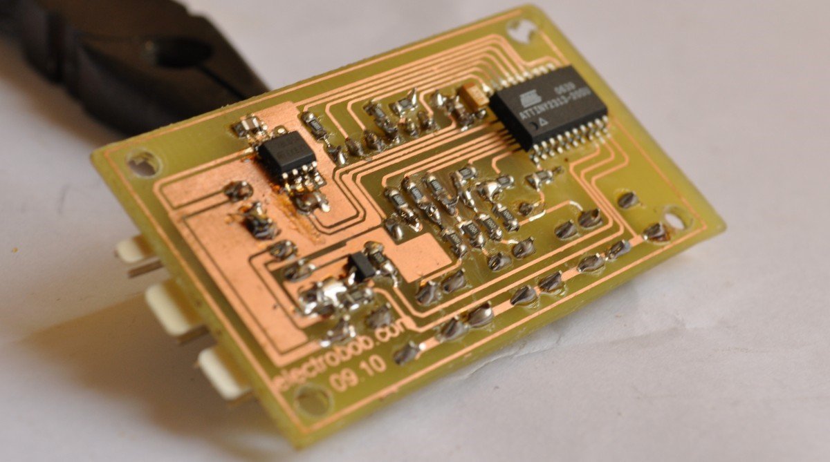
Once the drilling has been done, now the Printed Circuit Board is ready to be mounted with the electronic components which are required as per the requirement of the design and the specific requirement of the device the printed circuit board is supposed to be used in. Once all the components have been placed on the printed circuit board, they next stage is the soldering of the components so they remain in their place on their specific place for as long as the device has to work.
The soldering is done with the help of a solder and copper filler which is helped to solder the components.
The last step is then the cleaning and trimming of the printed circuit board so the debris and residual of the soldering can be removed as well as the components strands can be trimmed in order to avoid any short circuit issue in future for the printed circuit board (PCB).
Now if you want you can run some tests for analyzing the performance of the PCB. Some short circuit tests through meter and electrical tests are recommended before the operation of the PCB. Visual inspection tests can also be performed so that the components placed on the surface of the PCB are appropriately placed.
This tutorial has been prepared by SynergisePCB Inc. which is a commercial and leading manufacturer of PCBs in USA. SynergisePCB Inc. is a USA based company who’s all manufacturing and designing are done in the United States and at the same time we provide highly competitive rates to our customers. We deeply care about the quality and reliability of our products and have always met the international standards of quality for our products.