
Trace: It is a running path of copper on a printed circuit board. Through the traces, current can travel to different areas of the printed circuit board where the components are placed so that the desired action can be performed. In this article, we will discuss different types of traces on a Printed Circuit Board.
Some of the common traces are as follows:
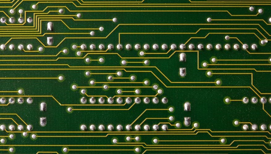
Traces on PCB
Traces are usually of two main type i.e. small and large trace.
- Small Trace: A small trace on a Printed Circuit Board connects the Reset pad to any other part of the printed circuit board.
- Large Trace: It connects the components to the 5V power pin.
V-score: It is a small cut through a printed circuit board. It allows the board to be snapped along a line conveniently.
Via: The different layers of the PCB are connected through via of various types depending upon the requirement. Some of the main types of via used in multi layer Printed Circuit Boards (PCB) are Plated through via, buried via hole and blind via hole.
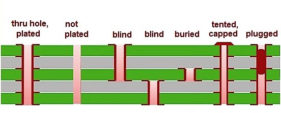
Plated through Via: Plated through via connects the top and the bottom layer of the multi layer Printed Circuit Boards (PCB). In order to spot a plated through hole, you can see if the light passes through it or it is possible to see through it. Plated through holes are the simplest kind of holes and they only need drilling or laser light to be drawn. Drilling of plated through holes is relatively cheap but they may take up more space as compared with the other types of via or the micro via.

Blind via hole (BVH): Blind via hole connects the outer layer of the PCB with the inner layers and it is not possible to see through the Blind via Hole (BVH) which is the reason why it derives its name. Blind via Hole is mostly used where the size and space utilization of the Printed Circuit Boards (PCB) is of importance. Blind via Hole are difficult to deal in as they require special attention to the depth of the hole to be made as anything imprecision in this regards can lead to severe design and operation complications. Due to the difficulty in handling them, the blind via Holes are not frequently used in the Printed Circuit Boards (PCB) assembly.
Buried Via Hole: The buried via Hole connects the inner layers of the Printed Circuit Boards (PCB) while it does not pass through the outer layer. The buried via holes are made use of where space utilization is important and high density applications are to be supported. The buried via holes are commonly used in HDI technology. Buried via holes are extremely difficult to work with as they require more time as compared with the blind via hole and the plated through hole technology while special care is required in working with them.
Micro Via: Micro via are another type of via used in the Printed Circuit Boards (PCB). They are via of very small size less than few micrometers and are used in highly sophisticated application. Micro-via are commonly used in flexible Printed Circuit Boards (PCB) or rigid flex Printed Circuit Boards (PCB).

Wave solder: It is a popular method of soldering that is used on printed circuit boards. In this technique, the board is moved over a stationary wave of molten solder. The molten solder adheres to pads that are visible and component leads on the printed circuit board.